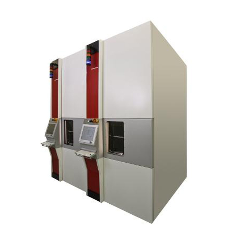
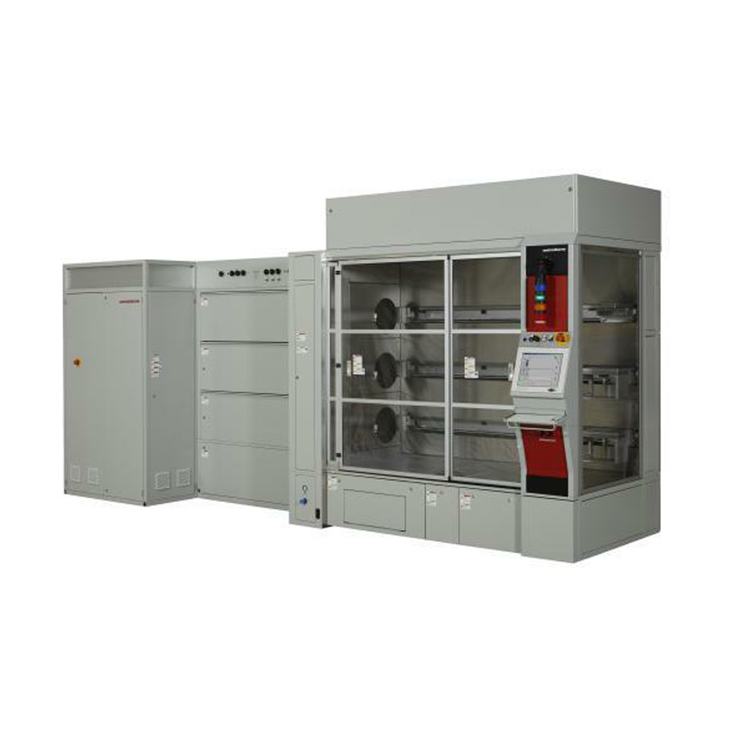
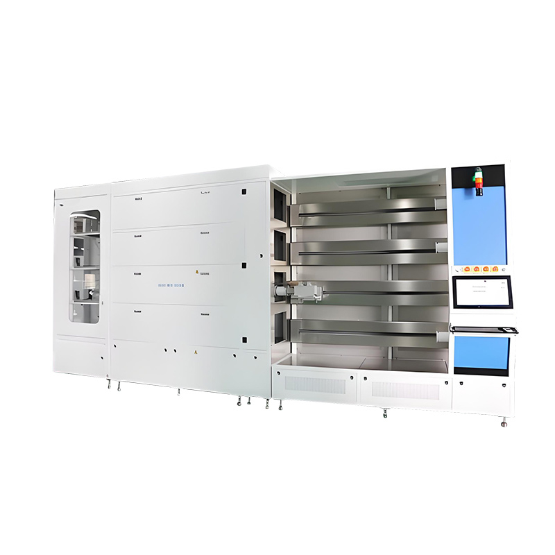
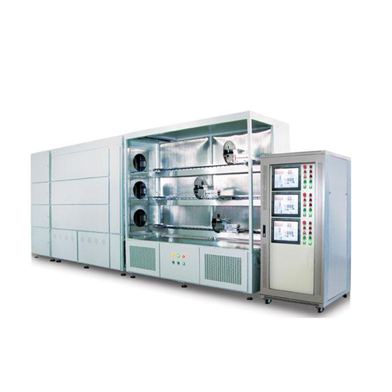
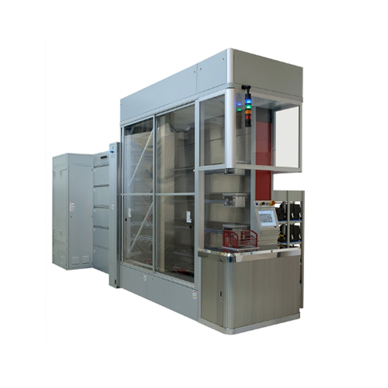
Chip diffusion furnace is one of the important process equipment of semiconductor production line, which is used for diffusion, oxidation, annealing, alloying and sintering of large-scale integrated circuit, discrete device, power electronics, photoelectric device and optical fiber industries.
There are two types of diffusion furnace: vertical diffusion furnace and horizontal diffusion furnace. Vertical diffusion furnace The vertical diffusion furnace is a quartz boat perpendicular to the horizontal plane, which is more conducive to the robot to transfer the silicon chip, and the process parameters in the chip are better consistent. Horizontal diffusion furnace Horizontal diffusion furnace is a quartz boat parallel to the horizontal plane, a can be 4 or more than 4 process furnace tubes, the average furnace tube covers a smaller area, the process parameters between the pieces is better than the vertical diffusion furnace.
Product characteristics
First, high precision and stability
High-precision control: The chip diffusion furnace is usually equipped with a high-precision temperature controller, which can achieve rapid and stable temperature control and meet the high-precision process requirements. For example, the control accuracy of some models of diffusion furnaces can reach ±1 ° C or even higher.
Temperature uniformity: Through advanced temperature control systems and furnace design, diffusion furnaces ensure uniform temperature distribution in the furnace, reducing the influence of temperature gradients on the process. For example, the temperature uniformity in the constant temperature zone of some diffusion furnaces can reach ±0.5℃/1080mm.
Second, multi-function and flexibility
Various process applications: The chip diffusion furnace can be used for the diffusion, oxidation, annealing, alloying and sintering of semiconductor materials.
Customized design: The diffusion furnace can be customized according to customer needs, including the adjustment of furnace size, heating zone length, temperature zone points and other parameters to meet different process requirements.
Third, high efficiency and energy saving
Fast heating speed: Diffusion furnaces usually use advanced heating elements and efficient heating methods, which can quickly heat up to the required temperature and shorten the process cycle.
Energy saving design: By optimizing the furnace structure and heating element layout, the diffusion furnace can achieve maximum energy utilization and reduce energy consumption.
Fourth, environmental protection and safety
Environmental performance: The diffusion furnace pays attention to environmental performance in the design and use process, minimize the production of volatile substances, and reduce the impact on the heating chamber environment.
Safety protection: The diffusion furnace is equipped with multiple safety protection measures, such as alarm protection over temperature, under temperature, broken couple, as well as protection of the safe temperature of the furnace door and the protection of the permission of the thermostat to open, etc., to ensure the safety of the equipment during use.
5. Advanced technology and innovation
New furnace body design: Adopt new furnace body design, such as FEC ceramic fiber tube insulation, KANTHEL furnace wire, etc., to improve temperature stability and service life.
Intelligent control system: Equipped with advanced microcomputer control system, PID closed-loop control temperature, to achieve a high degree of automation and intelligent control.
In summary, the chip diffusion furnace has the characteristics of high precision and stability, multi-function and flexibility, high efficiency and energy saving, environmental protection and safety, and advanced technology and innovation. These characteristics make the diffusion furnace play an irreplaceable role in the semiconductor manufacturing process, and continue to upgrade with the continuous development of manufacturing technology.
Buy Information
If you are interested in our two-stage rotary vane vacuum pumps, please contact us for more information and quotation.
• Contact number: +8615617875939
• Email: gordon@zztainuo.com
• Contact: Gordon Zhang
• Wechat: 15617875939
• WhatsApp: +8613592553141
Technical parameters:
Requirements | Specific specifications |
Model number | SE-CY-8A |
Silicon Wafer size | 8 inches |
Craft | Oxidation process |
Requirements for the boat | 1 boat position |
Make piece quantity | ≥ 50 tablets/lot |
Number of tab let rack stores | 4 piece rack locations |
Operating system | Ch inese or Eng l ish W indows operation |
Body s ize of equipment | Depth (4000mm) * Width (1000mm) * Height (3260mm) |
Main controller | SHARE2020 |
Data Records | Recipe management, alarm information query, historical operation information query |
Three leve ls of authority management | ( OP , E n g i neer , A dm i n ist rato r) |
Temperature controller | 4 or 5 point, thyristor temperature control |
Temperature check of furnace tube | Automatic temperature calibration |
Process gas | (Subject to customer confirmation) : N2 specific gas route configuration shall be subject to the technical specifications |
MFC brand | NAura |
MFC Precision | Plus or minus 1% |
Heating furnace body | High temperature furnace body |
Maximum operating temperature | 1000C |
Process temperature | 1000°C (±0.5 °C) |
Heat controlled thermocouple | 4 or 5 single set type R thermocouples |
Super warm thermocouple | 4 or 5 single set type R thermocouples |
Laween distribution thermocouple | Four or five o 'clock |
Furnace body constant temperature zone | 820 mm or higher |
Heating rate | > 10 ℃ / min |
Cooling rate | > 2 ℃ / min |
Efficient part | Silicon wafer loading and unloading area, flower basket storage area and flower basket entrance area are configured |
Cooling water flowmeter and sensor | Configure cooling water regulating valve and alarm contact |
Air disc and air road | No leak point |
Failure rate of film transfer | Continuous loading and unloading 10 furnace, no fault |
Granules | 0.3μm≤30 PCS (thousandth environment) |
Wafer breakage | < 1:10,000 |
Online time | 95% or higher |
Mean time between failures | >1000hr |
Average repair time | <8hr |
Hard drive | So l id state dua l hard dr ive, capacity no less than 500G, w ith rea l-t ime mutua l backup function ; |
Monitor | No less than 15.6 inches, touch screen |
Computer configuration | CPU: No less than I5, memory: no less than 8GB |
SECS/ GEM | Reserved interface |
Main Components:
Part name | Part description |
Equipment host | Tube furnace |
Mechanical pump | One |
A water cooler | One |
Random accessories | A set |
User manual | A copy |
Application field:
The application areas of the chip diffusion furnace are mainly concentrated in semiconductor manufacturing and related industries, and the following are its main application areas:
1. Semiconductor chip manufacturing:
Diffusion furnace is one of the important process equipment in the pre-process of semiconductor production line, which is mainly used to diffuse doped materials into silicon wafers to form PN structure. PN junction is the basic component of semiconductor device, its performance depends on the electrical parameters of PN junction, such as doping concentration, doping depth, resistivity and so on. Diffusion furnace is one of the key equipment to realize these performance parameters.
2. Solar cell manufacturing:
In the solar cell manufacturing process, diffusion furnaces can be used to prepare metal/semiconductor contacts and control the contact resistance, thereby improving the performance and efficiency of the solar cell.
3.LED device manufacturing:
Diffusion furnaces are also used in the field of LED device manufacturing to achieve specific doping processes to meet the electrical and optical performance requirements of LED devices.
4. Large-scale integrated circuit:
The diffusion furnace is not only used for doping process, but also for oxidation, annealing, alloying and sintering of large-scale integrated circuits, providing key support for the manufacture of integrated circuits.
5. Discrete devices, power electronics, optoelectronic devices and optical fiber:
Diffusion furnaces also play an important role in these industries, enabling a variety of key process steps to improve product performance and reliability.
In summary, chip diffusion furnaces have a wide range of applications in semiconductor manufacturing and related industries. With the continuous development of electronics, energy and other fields, diffusion furnace technology is also constantly innovating and evolving, and will continue to play an important role in semiconductor, solar cells, LED devices and other fields.
Application Case Introduction to the process of deposition of silicon nitride film thickness of 0.5μm on the surface of 4-inch wafer using chip diffusion furnace
Use a chip diffusion furnace to deposit a 0.5μm thick silicon nitride (Si3N4) film on the surface of a 4-inch wafer, roughly as follows:
First, the preparation stage
1. Wafer pretreatment:
Choose a 4-inch wafer size as the base.
The wafer is cleaned to remove impurities and contaminants from the surface and ensure the quality of the deposited film.
2. Equipment Preparation:
Check the cleanliness and integrity of the chip diffusion furnace to ensure that the equipment is in good condition.
Adjust equipment parameters, such as temperature, gas flow, etc., according to the requirements of deposition of silicon nitride film.
Second, sedimentary stage
1. Heating and gas intake:
The wafer is placed in the chip diffusion furnace and heated to the appropriate deposition temperature.
Through the reaction gases, such as silane (SiH4) and ammonia (NH3), these gases will chemically react at high temperatures to form a silicon nitride film.
2. Chemical reaction and film growth:
At high temperatures, silane and ammonia molecules come into contact with the wafer surface through convection and diffusion, and are adsorbed on it.
These gas molecules chemically react on the wafer surface to form a solid film of silicon nitride.
With the increase of deposition time, the thickness of the silicon nitride film gradually thickens until the desired thickness of 0.5μm is reached.
3. Monitoring and adjustment:
During the deposition process, the deposition rate and film thickness need to be monitored in real time to ensure the stability and controllability of the deposition process.
According to the monitoring results, timely adjust the parameters of the equipment, such as gas flow, temperature, etc., to optimize the deposition effect.
Third, post-processing stage
1. Cooling and removing:
After the deposition is complete, the chip diffusion furnace is gradually cooled to room temperature.
Remove the wafer and conduct subsequent processing and testing.
2. Detection and evaluation:
The thickness, uniformity and compactness of the deposited silicon nitride films were measured.
Evaluate the properties and quality of the film to ensure that it meets the requirements of the subsequent process.
Fourth. Precautions
1. Safe operation:
In the entire deposition process, it is necessary to strictly follow the safety operation procedures to ensure the safety of personnel and equipment.
2. Equipment maintenance:
Regular maintenance and maintenance of the chip diffusion furnace to ensure the stability and reliability of the equipment.
3. Process optimization:
According to the actual demand, the deposition process parameters are constantly optimized to improve the quality and performance of the film.
In summary, using the chip diffusion furnace to deposit 0.5μm thick silicon nitride film on the surface of a 4-inch wafer needs to go through several steps such as preparation stage, deposition stage and post-treatment stage. At each stage, strict control of process parameters and operating procedures is required to ensure that high-quality silicon nitride films are deposited.

